
TSMC A16 vs Intel 18A: The Angstrom Node Revolution in 2026
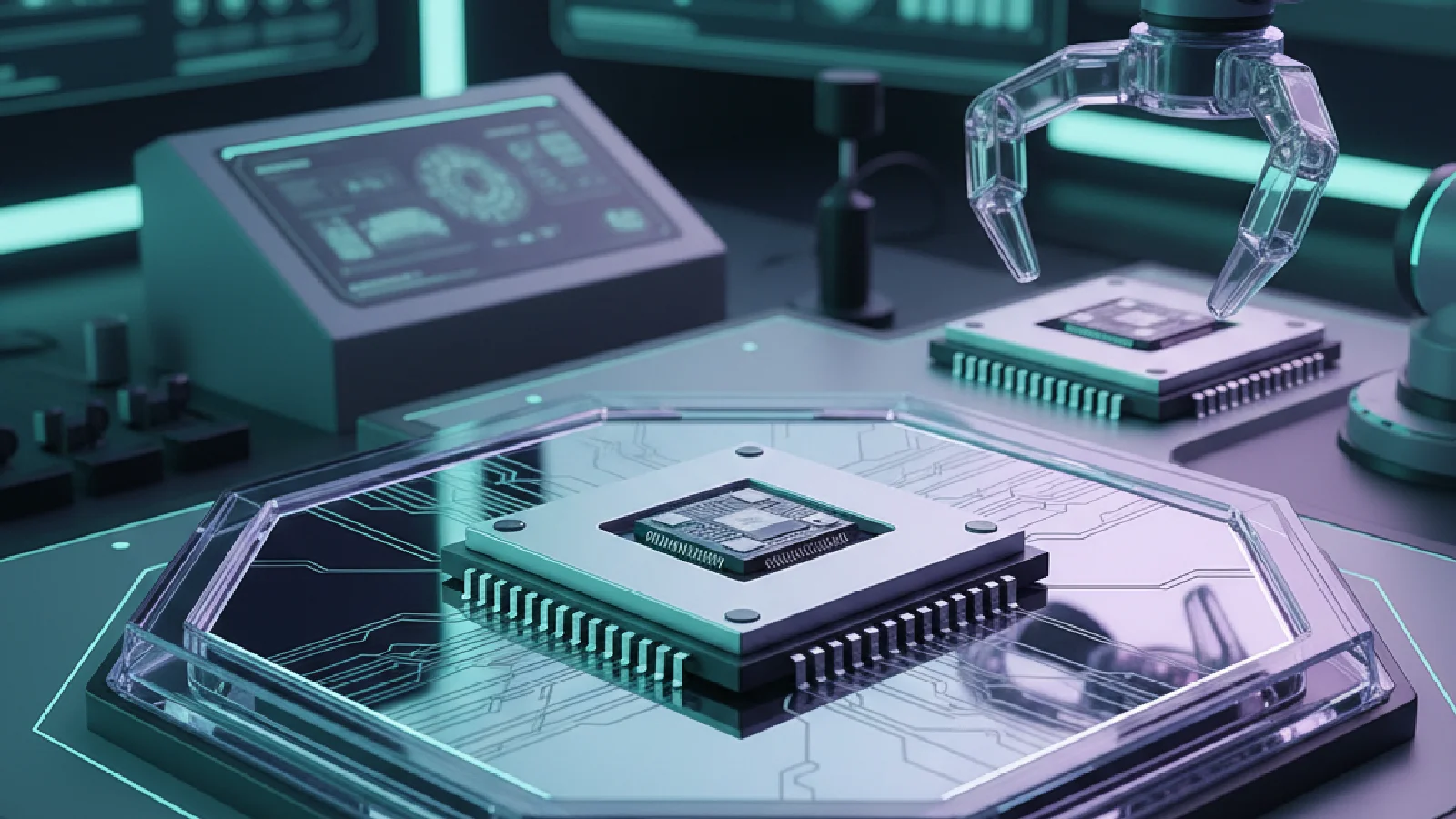
The semiconductor industry is reaching a historic milestone in 2026 with the official entry into the Angstrom era. This transition marks a decisive turning point where transistor dimensions are now measured in units smaller than a nanometer. At the heart of this technological revolution, two giants are clashing: Intel with its 18A node (1.8 nm) and TSMC with its A16 process (1.6 nm).
This technological battle goes beyond a simple engineering challenge. It will determine who controls the silicon foundations of tomorrow's artificial intelligence and will shape the technological ecosystem of 2026-2030. For the first time in over a decade, Intel seems to have a real chance to rival TSMC's dominance.
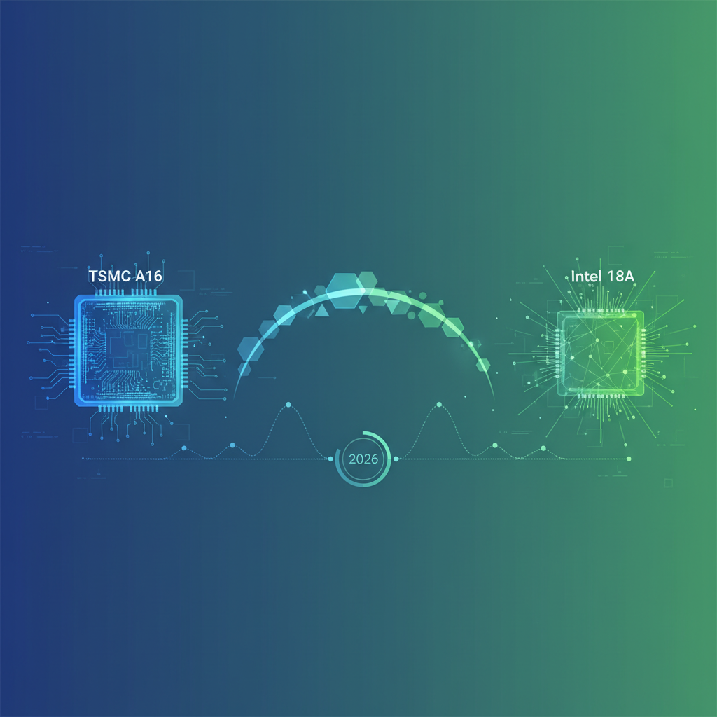
Intel 18A: The Technological Bet on a Resurgence
Intel officially began volume production of its 18A node in its Fab 52 in Arizona in early 2026. This technology represents the culmination of the "Five Nodes in Four Years" strategy initiated to regain technological leadership lost to TSMC.
Revolutionary RibbonFET Architecture
The 18A node relies on RibbonFET Gate-All-Around (GAA) transistors, an architecture that completely surrounds the conductive channel for optimal electrical control. Combined with the PowerVia innovation (backside power delivery), this configuration delivers:
- 50% performance/watt improvement compared to the previous generation
- Yields progressing towards 70-75% according to industry sources
- A slight lead over TSMC's N2 node in normalized performance per transistor
The PowerVia architecture represents a major breakthrough by moving power connections under the substrate, freeing up space above to optimize signal interconnections. This approach allows Intel to claim substantial gains in effective density and energy efficiency.
TSMC A16: The Controlled Evolution of the Dominant Ecosystem
For its part, TSMC is preparing its response with the A16 node (1.6 nm), scheduled for volume production in the second half of 2026. This technology is part of the N2 → N2P → A16 roadmap, capitalizing on expertise accumulated with decentralized cloud technologies and the AI ecosystem.
Comparative Technical Specifications
The battle is being fought on several crucial technical fronts:
| Criterion | Intel 18A | TSMC A16 |
|---|---|---|
| Transistor Density | Baseline | +10-12% vs 18A |
| Energy Efficiency | 50% improvement | +10-15% vs 18A |
| Transistor Architecture | RibbonFET GAA | Nanosheet GAA |
| Backside Power Delivery | PowerVia | Super Power Rail |
| Yields | 70-75% | 60%+ (historically stable) |
TSMC is betting on nanosheet GAA transistors combined with Super Power Rail, an evolution of its proven approach that prioritizes yield stability and gradual ramp-up.
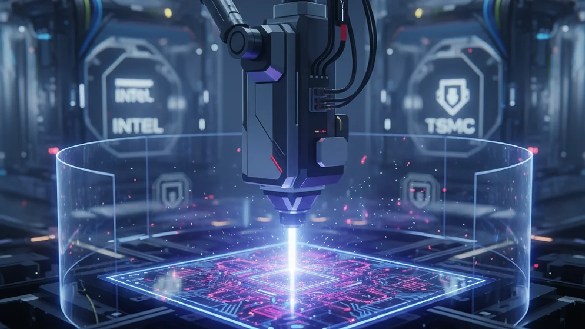
Strategic Implications for the Technological Ecosystem
Intel: Diversification and Reconquest
Intel's strategy revolves around several axes:
- Dedicated AI processors: Panther Lake and Clearwater Forest Xeon directly leverage 18A
- Supply-chain diversification: Hyperscalers seek to reduce their dependence on TSMC
- Open Foundry: Intel Foundry Services offers 18A to external clients
This approach allows Intel to play the card of a geopolitical alternative to TSMC's Taiwanese concentration, particularly attractive to American and European players.
TSMC: Volume and Mature Ecosystem
TSMC maintains its structural advantages:
- Massive production capacity: 200,000 wafers/month projected by 2030
- Diversified customer ecosystem: Apple, NVIDIA, AMD, Qualcomm
- Accumulated expertise: Mastered technological transitions over several generations
"The competition inaugurates the Angstrom era, with Intel aiming to use 18A as a springboard to its 14A high-NA EUV node to regain process leadership, while TSMC leverages the N2 → N2P → A16 roadmap to maintain its dominant market share." - MarketMinute Analysis
Technological Challenges and Physical Limits
The race towards Angstrom reveals fundamental physical challenges that the two players are tackling differently.
Increasing Manufacturing Complexity
- High-NA EUV lithography: Intel is investing heavily in this technology for 14A
- Defect control: Each generation multiplies potential sources of error
- Exponential costs: R&D investments exceed 20 billion dollars per node
This technological escalation creates an almost insurmountable barrier to entry for new players, consolidating the Intel-TSMC duopoly.
Target Applications and Segmentation
Both nodes are intended for specific markets:
Intel 18A focuses on:- High-performance server processors
- Edge computing AI solutions
- Applications requiring optimized CPU-GPU integration
- Massively parallel AI accelerators
- Premium mobile processors
- General-purpose high-performance computing
This specialization could lead to coexistence rather than exclusive domination, with each technology excelling in its preferred application domain.
Impact on the AI Ecosystem and Beyond
Revolution in Computational Performance
The simultaneous arrival of the 18A and A16 nodes catalyzes several transformations:
- More complex AI models: Gains in energy efficiency allow for more sophisticated neural architectures
- Edge computing: Miniaturization allows AI to be integrated into energy-constrained devices
- Hybrid quantum computing: These nodes could serve as an interface with emerging neural implant technologies
Geopolitical Repercussions
The technological battle between Intel and TSMC transcends industrial competition to become an issue of technological sovereignty. Europe and the United States are investing massively to reduce their dependence on Asia for advanced semiconductors.
Future Roadmap: Towards 14A and Beyond
2027-2030 Vision
Intel plans to use 18A as a springboard to its 14A node (1.4 nm) leveraging high-NA EUV lithography. This technology promises substantial additional gains in density and performance.
TSMC is simultaneously developing its post-A16 roadmap, with even more advanced nodes potentially integrating more complex 3D architectures and alternative materials to silicon.
This innovation race raises the question of economic sustainability: exponential development costs require colossal production volumes to be amortized, favoring industrial concentration.
Thus, 2026 marks a decisive turning point where semiconductor physics pushes its ultimate limits. Intel and TSMC, each with its distinct strategy, are shaping the technological architecture that will power artificial intelligence and high-performance computing for the coming decade.
This Angstrom node battle perfectly illustrates how the most invisible innovations – a few atoms gained or lost in a transistor – determine technological capabilities on a global scale. Far from being a simple technical race, it redefines geopolitical and industrial balances for the years 2026-2030.